Theory — Logic Gates and ICs
Back to Electronics hub GlossaryLogic gates and truth tables, the control circuits you must be able to describe (op-amp comparator and the 555), and the IC pin-outs on the data sheet.
Logic gates & truth tables
Key words
- Logic gate
- a part that gives a 1 or 0 output from 1/0 inputs.
- Truth table
- a table of every input and the output it gives.
- Combinational
- gates joined so one gate's output feeds the next.
A logic gate takes digital inputs (1/0) and gives a digital output set by its truth table. You must identify a gate from its symbol or truth table and complete a truth table. The symbols below are the distinctive shapes (the IEC operator is in brackets).
Combinational logic — work out the intermediate level first. Gates can be chained (up to 4 inputs, 2 outputs). Here an AND gate gives the intermediate signal G = A AND B, then an OR gate gives the output F = G OR C. Fill the G column before the output — exactly what the exam's "complete the truth table" question expects.
| A | B | C | G = A·B | F = G + C |
|---|---|---|---|---|
| 0 | 0 | 0 | 0 | 0 |
| 0 | 0 | 1 | 0 | 1 |
| 0 | 1 | 0 | 0 | 0 |
| 0 | 1 | 1 | 0 | 1 |
| 1 | 0 | 0 | 0 | 0 |
| 1 | 0 | 1 | 0 | 1 |
| 1 | 1 | 0 | 1 | 1 |
| 1 | 1 | 1 | 1 | 1 |
An AND gate gives an output of 1 only when inputs are 1. An OR gate gives 1 when input is 1. A NOT gate its input.
A system has two outputs from inputs A and B: X = A AND B and Y = A NOR B. Complete both output columns for all four input rows.
Answer
✅ You can now…
- identify a gate from its symbol or truth table.
- complete a truth table, working out any in-between level first.
Control circuits you must describe
Key words
- Comparator
- an op-amp that compares a signal with a set reference voltage.
- Astable
- a circuit that switches by itself — a continuous square wave.
- Monostable
- one trigger gives one output pulse of a fixed length.
You should be able to give a short "how it works" description for each of these circuits — and recognise the circuit diagram. All resistors are drawn the UK (BS) way, as a rectangle. The transistor switch is the fourth circuit you must describe.
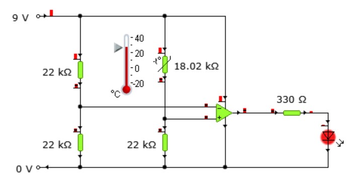
Op-amp comparator. The op-amp compares two voltages: a sensor divider on one input and a set reference level on the other. When the sensor voltage rises above the reference, the output swings high (LED on); below it, the output is low. This switches an output at a chosen light or temperature level.
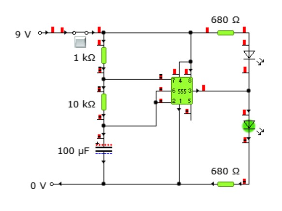
555 astable. With no trigger needed, the 555 runs continuously: C charges through R1 + R2 and discharges through R2, so pin 3 gives a steady square wave that switches between high and low. Bigger R or C values make it slower (lower frequency) — a flashing-LED or tone circuit.
555 monostable. It has one stable state. A short trigger pulse on pin 2 makes pin 3 go high for one fixed time set by R and C (a longer time for bigger R or C), then it returns low on its own — a one-shot timer (e.g. a timed light).
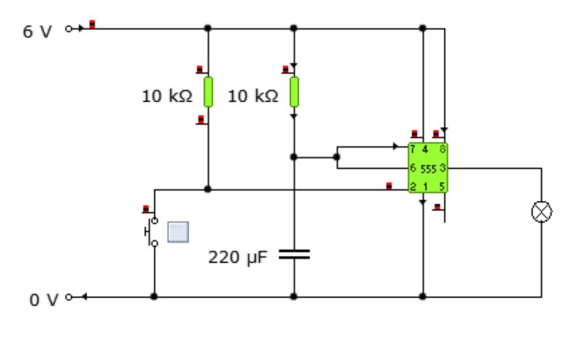
A 555 is wired so that one push of a button makes an LED stay on for exactly 5 seconds, then it goes off on its own. Is this an astable or a monostable, and what two components set the 5-second time?
Answer
✅ You can now…
- describe an op-amp comparator.
- describe a 555 astable and a 555 monostable, and say what sets their timing.
IC pin-out reference
Key words
- IC
- an integrated circuit — a "chip".
- Pin-out
- which job each pin (leg) of the chip does.
- Notch
- the mark that shows the pin 1 end of the chip.
These are the pin-outs given on the SQA data sheet, so you can recognise them in the exam and complete IC pin-out diagrams. The notch (or dot) marks the pin 1 end.
741 op-amp (8-pin)
555 timer (8-pin)
7408 — Quad 2-input AND
7432 — Quad 2-input OR
7400 — Quad 2-input NAND
7402 — Quad 2-input NOR
7486 — Quad 2-input XOR
7404 — Hex NOT (inverters)
On a 555 timer, which pin is the output, and on a 7408 AND-gate chip which pins are the power supply (Vcc) and ground (0 V)?
Answer
✅ You can now…
- read the 741, 555 and 7400-series pin-outs.
- find the power (Vcc) and ground (0 V) pins on a chip.
Logic Lord — build the truth tables
Fill in the output (Q) column for every gate. Tap a cell to cycle it through 0 and 1. Get every cell right to earn the 🚦 Logic Lord badge — completing the six Theory badges also unlocks 🎓 Theory Triumph.
Check your understanding
Answer the multiple-choice questions, then mark yourself with the RAG self-check.
RAG self-check
Tap Red / Amber / Green for how confident you feel.