555 Astable Simulator
Learning Goals
- Understand how R1, R2 and C1 set the flash rate
- Explain why LEDs flash alternately
- Relate the capacitor voltage curve to LED behaviour
- Link a stripboard layout to a circuit diagram
- Calculate Tm, Ts, T, f and duty cycle
Key Misconceptions
- The capacitor never reaches 0V or full supply voltage.
- R1 affects charge time but NOT discharge time.
- LEDs do not both connect the same way — one lights on HIGH, one on LOW.
- R1, R2, C1 change the timing non-linearly.
What this Page Is For
This page helps you understand, build, and test a 555 astable circuit. Use the tabs at the top to explore how it works, try the simulator, compare the schematic to a stripboard, and read a simple student explanation.
Move slowly, test often, and try each slider to see what changes.
How the 555 Astable Works
The most important idea: The capacitor does NOT fully charge or fully discharge. It moves only between 1/3 and 2/3 of the supply voltage.
Overview
The 555 astable creates a repeating HIGH–LOW output. The timing is controlled by three components:
- R1 – charge resistor
- R2 – charge & discharge resistor
- C1 – timing capacitor
🔼 Threshold & Trigger – the 1/3 and 2/3 rule
Inside the 555 are two voltage comparators:
- Upper comparator: switches the output LOW when the capacitor reaches 2/3 Vcc
- Lower comparator: switches the output HIGH when the capacitor falls to 1/3 Vcc
This causes the capacitor to “bounce” between these two levels forever.
⚡ Charging Phase – Output HIGH
When the output is HIGH:
- C1 charges through R1 + R2
- The voltage rises from 1/3 → 2/3 Vcc
- The green LED lights (on your circuit)
⬇ Discharging Phase – Output LOW
When the output is LOW:
- C1 discharges through R2 only
- Voltage falls from 2/3 → 1/3 Vcc
- The red LED lights
🧮 R1, R2, C1 Timing Equations
Mark (HIGH) time: Tm = 0.7 × (R1 + R2) × C1
Space (LOW) time: Ts = 0.7 × R2 × C1
Period: T = Tm + Ts
Frequency: f = 1 / T
🚫 Common Misconceptions Explained
- “R1 controls discharge time.”
False — only R2 is in the discharge path. - “The capacitor reaches full 0–Vcc.”
False — the comparators limit it. - “LEDs are symmetrical.”
False — they need opposite driving for HIGH/LOW light.
Interactive Simulator
Adjust R1, R2 and C1 to explore the 555 astable
This simulator shows the live behaviour of the 555:
- Real-time LED flashing
- Output HIGH/LOW state
- Charging/discharging phase
- Waveform output
- Capacitor voltage curve
- Calculated timing values
Everything updates instantly when you move the sliders.
LED Output
GREEN = Output HIGH (charging phase)
RED = Output LOW (discharging phase)
(pin 3 → 0V)
(Vsupply → pin 3)
Output State: —
Presets
Click a button to instantly load a timing setup.
Adjust Component Values
Move the sliders to change resistor and capacitor values. The flash rate and waveforms update automatically.
Output Square Wave
Capacitor Voltage Curve
Calculated Values
Period T: — s
Frequency f: — Hz
Mark Time Tm: — s (HIGH time)
Space Time Ts: — s (LOW time)
Duty Cycle: —%
Schematic & Stripboard
Both diagrams show the same circuit in different layouts.
The schematic shows the logical circuit.
The stripboard shows the physical layout.
Every electrical connection must match – even if the picture looks different.
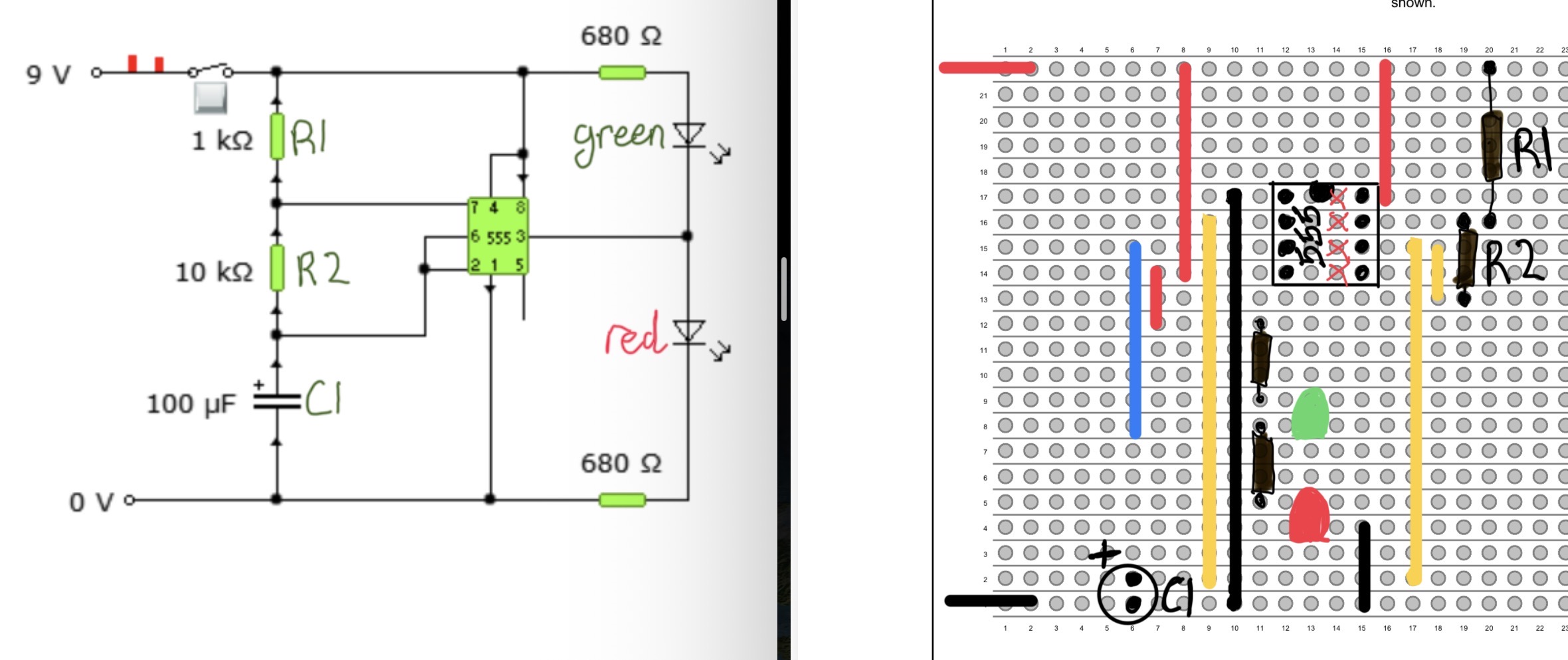
🔍 Spot the Difference — Schematic vs Stripboard
The pictures look different – but the connections are identical. Here’s what changes when moving from schematic → stripboard.
Key Differences
- Schematic is neat – wires avoid crossing, parts spaced out.
- Stripboard follows copper tracks – many parts end up rotated or moved.
- IC pins look different – but are still the same numbers.
- Components may swap sides of the chip.
What always stays the same
- Pin 2 and pin 6 must be linked (timing node).
- R1 and R2 must both connect to pin 7.
- C1 must go between the timing node and 0V.
- Pin 3 must drive the LEDs.
- +V must always go to pin 8.
If the schematic says two things join → they MUST join on the stripboard, even if the picture layout is very different.
📘 Key Comparison Notes
1. Pin Numbers NEVER change
Pin 1 is always the bottom-left of the notch. Count anticlockwise.
2. Timing node is the heart of the circuit
Pins 2 and 6 must be connected together AND go to R5 and C1.
3. LED wiring flips depending on HIGH/LOW driving
- Green LEDs turn on when pin 3 is HIGH
- Red LEDs turn on when pin 3 is LOW
4. Track cuts under pins
Every IC pin must sit on isolated copper.
5. Real boards look “messier” than diagrams
This is normal. Electrical connections matter — not neatness.
Build Guide – 555 Astable Stripboard
I can...
- Place the 555 IC the correct way around
- Wire the timing components correctly
- Check LED polarity
- Match every connection to the schematic
🧭 Step 1 — Place the 555 and mark pin 1
The 555 has a notch or a dot marking pin 1. Make sure this is at the top-left of the chip.
     Notch ↑
      ___
     |   |   ← 555 IC
 1 • |   | • 8
 2 • |   | • 7
 3 • |   | • 6
 4 • |___| • 5

Pin numbers go counter-clockwise.
- Pin 1 → 0V
- Pin 8 → +V
- Each pin must sit on its own copper strip
Common error: rotating the chip 180°. Always check pins 1 and 8.
🔌 Step 2 — Add the power rails (+V and 0V)
Use standard colour coding:
- Red = +V
- Black = 0V
Top of board:
+V  ───────────────────────────────

Bottom of board:
0V  ───────────────────────────────
+V must reach pin 8. 0V must reach pin 1.
⏱ Step 3 — Build the timing network (R4, R5, C1)
Connections
- R4 → +V → pin 7
- R5 → pin 7 → timing node (pins 2 & 6)
- C1 → timing node → 0V
      +V
       │
      [R4]
       │
      Pin 7 ─────[R5]─────┐
                          │
                      Pins 2 & 6
                          │
                         [C1]
                          │
                         0V
Polarity warning: C1 is electrolytic → long leg = timing node, short leg = 0V.
💡 Step 4 — Add the LEDs and resistors
Green LED (HIGH output)
Pin 3 ──[Resistor]──►|── 0V
                     LED
(►| = arrow points from + to –)
Red LED (LOW output)
+V ──[Resistor]──►|── Pin 3
                  LED
The flat edge of an LED = negative (–).
🖇 Step 5 — Add all required links
Any schematic connections not joined by copper tracks must be wired manually.
Most common links:
- Pin 2 ↔ Pin 6 (timing node)
- +V rail extensions
- 0V rail extensions
- Long cross-board connections
Pins 2 and 6:
   2 ─────────── 6
(Use a short wire link)
Use purple for timing node links (recommended colour convention).
✔ Step 6 — Full Build Check
- Pin 1 → 0V
- Pin 8 → +V
- Pins 2 & 6 joined
- R4, R5, C1 correctly connected
- C1 polarity correct
- LED polarity correct
- No pins share the same strip accidentally
If the LED does not flash:
- Check C1 orientation
- Check pins 2 & 6 are linked
- Check R4/R5 values
- Check correct pin numbering
Student-Friendly Explanation
This section explains the 555 astable in simple language. It is written for a reading age of 11–12 and uses clear, everyday ideas.
The Big Picture
The 555 makes a repeating ON–OFF signal all by itself. This is called an astable because it never stays still.
It keeps flashing between HIGH and LOW forever.
The Capacitor: The “Bucket” of Charge
Think of the capacitor like a bucket that fills and empties.
- When the bucket is filling → the output is HIGH
- When the bucket is emptying → the output is LOW
But it never fills all the way and never empties all the way — it goes between 1/3 full and 2/3 full.
What R1, R2 and C1 Do
- R1 controls how fast the bucket fills
- R2 controls filling AND emptying
- C1 is the size of the bucket
Bigger resistors → slower charging Bigger capacitor → longer flashes
Why the LEDs Flash
The output pin (pin 3) goes HIGH and LOW over and over.
- HIGH turns the green LED on
- LOW turns the red LED on
This creates an alternating flash.
What You Control
By changing R1, R2 or C1 you control:
- How fast the LEDs flash
- How long the HIGH part lasts
- How long the LOW part lasts
- The overall frequency
This is why the sliders in the simulator change the pattern instantly.
Why the 555 is So Useful
The 555 is one of the most used chips in electronics because it can:
- Make clocks and timers
- Blink LEDs
- Drive buzzers
- Generate repeating pulses
It is simple, cheap and reliable — perfect for learning electronics.
Quick Quiz – Test Your Understanding
Answer the questions below. Your score updates automatically. You can retry any question until it is correct.